Catalog
-
Catalog
- Agriculture
- Apparel
- Automobiles & Motorcycles
- Beauty & Personal Care
- Business Services
- Chemicals
- Construction & Real Estate
- Consumer Electronics
- Electrical Equipment & Supplies
- Electronic Components & Supplies
- Energy
- Environment
- Excess Inventory
- Fashion Accessories
- Food & Beverage
- Furniture
- Gifts & Crafts
- Hardware
- Health & Medical
- Home & Garden
- Home Appliances
- Lights & Lighting
- Luggage, Bags & Cases
- Machinery, Hardware & Tools
- Measurement & Analysis Instruments
- Mechanical Parts & Fabrication Services
- Minerals & Metallurgy
- Office & School Supplies
- Packaging & Printing
- Rubber & Plastics
- Security & Protection
- Service Equipment
- Shoes & Accessories
- Sports & Entertainment
- Telecommunications
- Textiles & Leather Products
- Timepieces, Jewelry, Eyewear
- Tools
- Toys & Hobbies
- Transportation
Filters
Search

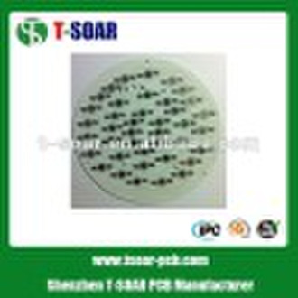
Circuit Diagram With PCB Process
original price: 0,30 USD
Shenzhen, China

Simon Liu
Contact person
Basic Information
| Place of Origin | Guangdong China (Mainland) |
|---|---|
| Brand Name | T-SOAR |
| Model Number | TS-010 |
Circuit Diagram With PCB Process, Circuit Drawing, Multilayers PCB. Welcome to T-SOAR PCB Manufacturer ----------------------------------------------------------------------------------------------------------- 1> PCB processingDetails: Place of Origin shenzhen China (Mainland) Brand Name: t-soar pcb Model Number: 2layers pcb Base Material: FR-4 Copper Thickness: 0.5oz Board Thickness: 2.4mm Min. Hole Size: 0.25mm Min. Line Width: 4mil Min. Line Spacing: 4mil Surface Finishing: OSP ( Lead Free) Soldermask: Black Legend: White Test: E-testing 2> Package & Delivery: Packing details: Heat sealed packing, vacuum packing, export carton Delivery time: 3-7days 3> Fabric Capacity: NO Item Craft Capacity1Layer1-30 Layers2Base Material for PCBFR4, CEM-1, TACONIC, Aluminium, High Tg MaterialHigh FrequenceROGERS ,TEFLON, ARLON, Halogen-free Material3Rang of finish baords Thickness0.21-7.0mm4Max size of finish board900MM*900MM5Minimum Linewidth3mil (0.075mm)6Minimum Line space3mil (0.075mm)7Min space between pad to pad3mil (0.075mm)8Minimum hole diameter0.10 mm9Min bonding pad diameter10mil10Max proportion of drilling hole and board thickness1:12.511Minimum linewidth of Idents4mil12Min Height of Idents25mil13Finishing TreatmentHASL (Tin-Lead Free), ENIG(Immersion Gold), Immersion Silver , Gold Plating (Flash Gold), OSP, etc.14SoldermaskGreen, White, Red, Yellow, Black, Blue, transparent photosensitive soldermask, Strippable soldermask.15Minimun thickness of soldermask10um16Color of silk-screenWhite, Black, Yellow ect.17E-Testing100% E-Testing (High Voltage Testing); Flying Probe Testing18Other testImpedanceTesting,Resistance Testing, Microsection etc.,19Date file formatGERBER FILE and DRILLING FILE, PROTEL SERIES, PADS2000 SERIES, Powerpcb SERIES, ODB++20Special technological requirementBlind & Buried Vias and High Thickness copper21Thickness of Copper0.5-14oz (18-490um) 4> Work Silhouette
Delivery terms and packaging
Packaging Detail: Heat Sealed Packing, Vacuum Packing, Professional Export Carton. Delivery Detail: 3-7 Days
Port: Shenzhen
Payment term
Documents Against Acceptance
Letter of credit
Telegraphic transfer
Western Union
-
Payment Methods
We accept:


