Catalog
-
Catalog
- Agriculture
- Apparel
- Automobiles & Motorcycles
- Beauty & Personal Care
- Business Services
- Chemicals
- Construction & Real Estate
- Consumer Electronics
- Electrical Equipment & Supplies
- Electronic Components & Supplies
- Energy
- Environment
- Excess Inventory
- Fashion Accessories
- Food & Beverage
- Furniture
- Gifts & Crafts
- Hardware
- Health & Medical
- Home & Garden
- Home Appliances
- Lights & Lighting
- Luggage, Bags & Cases
- Machinery, Hardware & Tools
- Measurement & Analysis Instruments
- Mechanical Parts & Fabrication Services
- Minerals & Metallurgy
- Office & School Supplies
- Packaging & Printing
- Rubber & Plastics
- Security & Protection
- Service Equipment
- Shoes & Accessories
- Sports & Entertainment
- Telecommunications
- Textiles & Leather Products
- Timepieces, Jewelry, Eyewear
- Tools
- Toys & Hobbies
- Transportation
Filters
Search

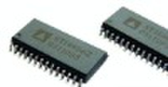
74LVC1G14GW - Single Schmitt-trigger inverter - NX
original price: 0,01 USD
Shenzhen, China
Production capacity:
1000000 Piece / Month

keiven wu
Contact person
Basic Information
| Place of Origin | Guangdong China (Mainland) |
|---|---|
| Brand Name | philips |
| Model Number | 74LVC1G17GV |
Philips Semiconductors Product specification Single Schmitt-trigger inverter 74LVC1G14 FEATURES · Wide supply voltage range from 1.65 V to 5.5 V · High noise immunity · Complies with JEDEC standard: – JESD8-7 (1.65 V to 1.95 V) – JESD8-5 (2.3 V to 2.7 V) – JESD8B/JESD36 (2.7 V to 3.6 V). · ±24 mA output drive (VCC = 3.0 V) · CMOS low power consumption · Latch-up performance exceeds 250 mA · Direct interface with TTL levels · Unlimited rise and fall times · Input accepts voltages up to 5 V · Multiple package options · ESD protection: – HBM EIA/JESD22-A114-B exceeds 2000 V – MM EIA/JESD22-A115-A exceeds 200 V. · Specified from -40 °C to +85 °C and -40 °C to +125 °C. DESCRIPTION The 74LVC1G14 is a high-performance, low-power, low-voltage, Si-gate CMOS device, superior to most advanced CMOS compatible TTL families. The input can be driven from either 3.3 V or 5 V devices. This feature allows the use of this device in a mixed 3.3 V and 5 V environment. Schmitt-trigger action at the input makes the circuit tolerant for slower input rise and fall time. This device is fully specified for partial power-down applications using Ioff. The Ioff circuitry disables the output, preventing the damaging backflow current through the device when it is powered down. The 74LVC1G14 provides the inverting buffer function with Schmitt-trigger action. QUICK REFERENCE DATA Ground = 0 V; Tamb = 25 °C; tr = tf £ 2.5 ns. Notes 1. CPD is used to determine the dynamic power dissipation (PD in mW). PD = CPD ´ VCC 2 ´ fi ´ N + S(CL ´ VCC 2 ´ fo) where: fi = input frequency in MHz; fo = output frequency in MHz; CL = output load capacitance in pF; VCC = supply voltage in Volts; N = total switching outputs; S(CL ´ VCC 2 ´ fo) = sum of the outputs. 2. The condition is VI = GND to VCC. SYMBOL PARAMETER CONDITIONS
Delivery terms and packaging
Packaging Detail: paper package Delivery Detail: 3days
Port: SHENZHEN
Payment term
Telegraphic transfer
MoneyGram
Western Union
-
Payment Methods
We accept:


