Catalog
-
Catalog
- Agriculture
- Apparel
- Automobiles & Motorcycles
- Beauty & Personal Care
- Business Services
- Chemicals
- Construction & Real Estate
- Consumer Electronics
- Electrical Equipment & Supplies
- Electronic Components & Supplies
- Energy
- Environment
- Excess Inventory
- Fashion Accessories
- Food & Beverage
- Furniture
- Gifts & Crafts
- Hardware
- Health & Medical
- Home & Garden
- Home Appliances
- Lights & Lighting
- Luggage, Bags & Cases
- Machinery, Hardware & Tools
- Measurement & Analysis Instruments
- Mechanical Parts & Fabrication Services
- Minerals & Metallurgy
- Office & School Supplies
- Packaging & Printing
- Rubber & Plastics
- Security & Protection
- Service Equipment
- Shoes & Accessories
- Sports & Entertainment
- Telecommunications
- Textiles & Leather Products
- Timepieces, Jewelry, Eyewear
- Tools
- Toys & Hobbies
- Transportation
Filters
Search

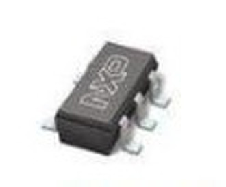
74LVC1G125GW - Bus buffer/line driver; 3-state - N
original price: 0,01 USD
Shenzhen, China
Production capacity:
1000000 Piece / Month

keiven wu
Contact person
Basic Information
| Place of Origin | Guangdong China (Mainland) |
|---|---|
| Brand Name | NXP |
| Model Number | 74LVC1G125GW |
NXP Semiconductors Product specification Bus buffer/line driver; 3-state 74LVC1G125 FEATURES · Wide supply voltage range from 1.65 V to 5.5 V · High noise immunity · Complies with JEDEC standard: – JESD8-7 (1.65 V to 1.95 V) – JESD8-5 (2.3 V to 2.7 V) – JESD8B/JESD36 (2.7 V to 3.6 V). · ±24 mA output drive (VCC = 3.0 V) · CMOS low power consumption · Latch-up performance exceeds 250 mA · Direct interface with TTL levels · Inputs accept voltages up to 5 V · Multiple package options · ESD protection: – HBM EIA/JESD22-A114-B exceeds 2000 V – MM EIA/JESD22-A115-A exceeds 200 V. · Specified from -40 °C to +85 °C and -40 °C to +125 °C. DESCRIPTION The 74LVC1G125 is a high-performance, low-power, low-voltage, Si-gate CMOS device, superior to most advanced CMOS compatible TTL families. The input can be driven from either 3.3 V or 5 V devices. This feature allows the use of this device in a mixed 3.3 V and 5 V environment. This device is fully specified for partial power-down applications using Ioff. The Ioff circuitry disables the output, preventing the damaging backflow current through the device when it is powered down. The 74LVC1G125 provides one non-inverting buffer/line driver with 3-state output. The 3-state output is controlled by the output enable input (OE). A HIGH level at pin OE causes the output to assume a high-impedance OFF-state. QUICK REFERENCE DATA GND = 0 V; Tamb = 25 °C; tr = tf £ 2.5 ns. Notes 1. CPD is used to determine the dynamic power dissipation (PD in mW). PD = CPD ´ VCC 2 ´ fi ´ N + S(CL ´ VCC 2 ´ fo) where: fi = input frequency in MHz; fo = output frequency in MHz; CL = output load capacitance in pF; VCC = supply voltage in Volts; N = total switching outputs; S(CL ´ VCC 2 ´ fo) = sum of the outputs. 2. The condition is VI = GND to VCC. SYMBOL PARAMETER CONDITIONS TYPICAL UNIT tPHL/tPLH propagation delay input A to output Y V
Delivery terms and packaging
Packaging Detail: paper package Delivery Detail: 3days
Port: SHENZHEN
Payment term
Telegraphic transfer
MoneyGram
Western Union
-
Payment Methods
We accept:


