Katalog
-
Katalog
- Auto & Motorrad
- Bauwesen und Immobilien
- Bekleidung
- Büro- und Schulartikel
- Chemikalien
- Dienstleistungen für Unternehmen
- Eisenwaren
- Elektrische Geräte & Zubehöre
- Elektronische Bauteile
- Energie
- Galanteriewaren
- Geschenke und Kunsthandwerke
- Gesundheit und Medizin
- Gummi und Kunststoffe
- Haus und Garten
- Haushaltsgeräte
- Koffer, Taschen & Hüllen
- Landwirtschaft
- Lebensmittel und Getränke
- Licht und Beleuchtung
- Maschinen, Geräte und Werkzeuge
- Maschinenteile und Herstellung Dienstleistungen
- Messapparat und Analysegerät
- Mineralien und Metallurgie
- Möbel
- Schuhe und Accessoires
- Schönheit und Körperpflege
- Service Geräte und -Ausstattung
- Sicherheit und Schutz
- Spielzeuge und Hobbys
- Sport und Unterhaltung
- Telekommunikations
- Textil und Lederware
- Transport
- Uhren, Schmuck, Brillen
- Umweltschutz
- Unterhaltungselektronik
- Verpacken und Drucken
- Werkzeuge
- Überschüssiger Warenbestand, Lager
Filters
Search

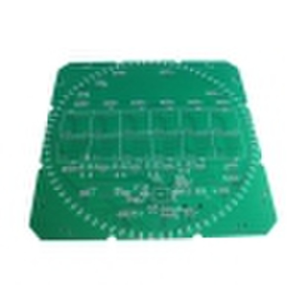
4 Schichten Leiterplatten
original-Preis: 110,00 USD
Shenzhen, China

Yoyo Dong
Kontaktperson
Basisdaten
| Ort der Herkunft | Guangdong China (Mainland) |
|---|---|
| Marke | CU |
| Modell-Nummer | N/A |
Multilayer PCBsCountry of Origin:China (mainland)Vendor to be UL recognized to minimum category of 94V0Fabricated in accordance with IPC-A-600,latest version unless otherwise specified in attached specification.All patterns according to Customer PCB Artwork/Film/Gerber File.Material: FR-4 We would provide a copy of UL materials certificate.This is a Single Layer Double Layer 4Layer OtherWeight of Copper: 1 oz per sq .ft(Base Material)for Outer Layers. Finish to be 2oz per sq.ft oz per sq.ft(Base Material)for Inner Layers.Finished Board thickness shall be(Tolerance is ±10%):0.8mm 1.0mm 1.2mm 1.6mm OtherFinishing according to IPC-TM-650(2.2.13)latest version.Via Method: PTH NPTH Blind Via between layerPCB must be identified with MFR’S approval logo, type designation week and year(WWYY) OF MFR and Customer P/NMFR’s UL Logo&indicated location According to PCB Drawing of Gerber dataDate code location: Print on Top/Bottom Side Silkscreen LayerEtch on Top/Bottom Side Copper Layer.Customer Part No.&Silkscreen Layers According to PCB Drawing or Gerber data indicated location.All PCB will be electrical tested before shipmentOther Test and Reliability standard refer to IPC-A-600(latest version)PCB Class1 Class2 Class 3As per ion-contamination test results.(IPC-TM-650 Test Method2.3.25)Finishing: HAL ENTEK Pre-flux Gold Flash Gold Plating Immersion Tin Immersion Silver Immersion goldMin. hole size: 12mil or mm(Remark: The minimum hole size are for drill bit size)Legend Silkscreen: Top or Bottom sideLegend marking do not allow printed on soldering pad and must keep clearance 10 mil min,leave to the soldering padSilkscreen color: White Yellow BlackWe will provide specification & Materail Safety Data Sheet(MSDS) of legend inkSoldermask: Wet film Dry film Conventional PeelablePlug all via holes by soldermask on Top Side or Bottom SideSoldermask color: Green Blue Yellow Red OtherFabrication: Routing Punching HandmadeAll sample board and risk buy order will be acceptable for routingPCB Unit/Panel size:163.3X215.6inch/mmComply RoHS standardPacking: PCB must be cleaned and dried to insure storage for 180 days in the unit package without corrosion, visible fingerprints, oxidation, mold or loss of solder ability. All boards shall be packaged in such a manner as to prevent board-to-board damage and/or damage from external cause. Paper interleaving is preferred, and if used, must be free of sulfites and other materials which will contaminate the board surface.Pattern Comparison :All patterns according to PCB Artwork/Film/Gerber File.Trace & Space Width Within ±20% per artwork.Conductor Nicks, scratches or pinholes < 20% of nominal widthPads :Nicks, scratches or pinholes < 20% of nominal width No lifted or damaged pad No dewetting, excessive solder or exposed copper for HAL .No decoloration, oxidation or exposed base metal for Au No scratch or exposed copper for carbon .Holes No block hole or extra hole on board No crack or excessive solder inside hole for PTH Annual ring, 0.1mm Min. for component hole and 0.05mm Min. for via hole No plating on Non-PTH wallSolder Mask ,No scratch, conductor exposed or foreign matter under solder mask.Solder mask on edges of non-soldering pads remains 80% of pad area.Solder mask on edges of soldering pad remains 80% of pad area for silk-screen method.No solder mask on all soldering pads for wet film method.No solder mask on all soldering pads except pad edges for all methods.Qualified and confirmed to requirement of IPC-SM-840, Class 2.Minimum thickness should be 0.0004 In. (0.01mm).Legend No illegible marking, mis-alignment or missing/extra marking No on pad except PTH Registration must be within 0.010 In. (0.25mm) of the silkscreen master pattern.Epoxy ink must be nonflammable,non-conductive, non-hydroscopic and able to withstand the wave soldering or SMT reflow soldering and post cleaning operation. Contact Finger No defect found on the central portion of the 80% finger area No Solder and Soldermask allowed on Contact Finger. Not allow exposing Nickel or Copper Base Material on Contact Finger.Electrical Test :No open/short circuits (Must be test in PP samples) All conductor paths must be tested for continuity and for shorts to all other conductors.The nets must be tested continuity at the plated through hole or surface mount pads.The maximum resistance must be 10 ohms or less.The minimum resistance must be 1M ohms at 100VDC or 2M ohms at 250VDC.E-test Mark Must be present after Electrical Test.Hole Sizes :Guide Holes -Measuring all, all according to Fab Dwg. PTH -Sampling at least 10 of evenly distributed holes of each hole size, all according to Gerber file or hole charts.NPTH -For punch holes, the tolerance ±0.1mm. For drill holes, the tolerance ±0.05mm.Outline Dimensions: All dimensions according to Fab DwgGuide Holes Locations: All guide holes locations according to Fab DwgBoard Edge Finish: Routing – All board edges must have a 125 RMS finish or batter. Copper is not allow on board periphery except at contact area of bevel. Punching – All board edges must have a finish clean and free of debris. Copper is not allowed on PCB periphery.Board Thickness: All thickness according to Fab Dwg.V-Cut: Distance of 2 V-Cut tips along H-plane of PCB <= 0.1mm Distance of 2 V-Cut tips along V-plane of PCB <= 1/3 T, where T = thickness of PCB, unless otherwise specified by Fab DrawingBow and Twist: Placing both sides in a flat surface, the highest point of both sides to the diagonal length < 1% for non-SMT and < 0.75% for SMT PCBs.Conductor Thickness Evaluation (Micro section or Radioactive Equipment): PTH wall and trace Cu finishing thickness > 0.025mm Pb/Sn thickness > 0.002mm (HAL) Au thickness > 0.076µm (Au PCB) > 0.76µm (Au finger) Ni thickness > 1.3µm (Au PCB) > 3.8µm (Au finger)Solvent Resistance: IPC-TM-650 (2.3.23) No attackAbrasion of Solder mask: IPC-TM-650 (2.4.27) Over 6HAbrasion of Solder mask: IPC-TM-650 (2.4.28) No peel offAdhesion of Silk-screen: IPC-TM-650 (2.4.1) No peel offSolder ability: ANSI/J-STD-003 100% for Non-SMT, 95% for SMTThermal Stress: IPC-TM-650 (2.6.8) No crack and delaminationCurrent Carrying Capacity: IPC-TM-650 (2.2.13) 2A min. for 3 minutesPull Strength of Conductor: IPC-TM-650 (2.4.8) => 1.25 kg/cm² widthPull Strength of PTH : IPC-TM-650 (2.2.13) => 140 kg/cm²Payment Terms: T/T or L/C30% Deposit and 70% before DeliveryMinimum Order: 1,0 to 1,000 Pieces
Lieferbedingungen und Verpackung
Packaging Detail: vacuum package, handwork packageOuter packing: carton Delivery Detail: 15days
Hafen: HONGKONG
Zahlungsbedingungen
Letter of credit
Telegraphic transfer
-
Zahlungsarten
Wir akzeptieren:


