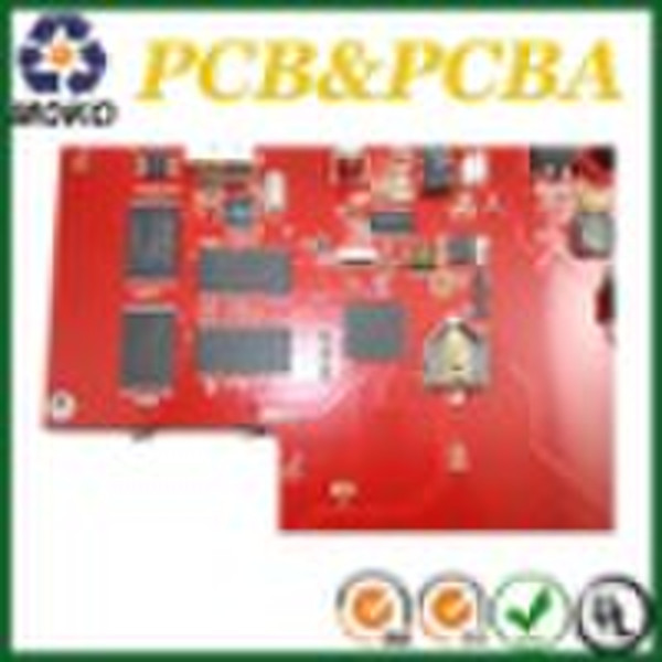
SMT 2 Layer PCBA Board
原价: 10,00 USD
深圳宝安国际机场, 中国

Sandy Xia
联系人姓名
基本信息
| 出生地 | Guangdong China (Mainland) |
|---|---|
| 牌子的名字 | MK |
| 模式的数量 | mkpcb000137 |
Welcome to Moko 2 layer pcba board Multi-layer pcba board pcb board,circuit board,electronic circuit, pcb layout,pcb design,rigid pcb,clone pcb,mcpcb,circuit layout Ourpcb assembly got UL,SGS,ROHS,ISO9002 cerfitifcates,and are used to a wide range of fields such as computers,digital porducts, medical equipment,automobiles, communication devices,military, industrial control and aviation.PCB Specification providing OEM service to all sorts of printed circuit board assembly 1 Layer 1-30 layer 2 Material FR-4,CEM-1,CEM-3,Hight TG,FR4 Halogen Free,FR-1,FR-2 3 Board thickness 0.2mm-7mm 4 Max.finished board side 1500mm*500mm 5 Min.drilled hole size 0.5mm 6 Min.line width 0.075mm(3mil) 7 Min.line spaceing 0.075mm(3mil) 8 Surface finish/treatment HALS/HALS lead free,Chemical tin,Chemical Gold,Immersion gold Inmersion Silver/Gold,Osp,Gold Plating 9 Copper thickness 0.5oz Min.,5.0oz Max 10 Solder mask color green/black/white/red/blue/yellow 11 Inner packing Vaccum packing,Plastic bag 12 Outer packing standard carton paking 13 Hole tolerance PTH:±0.076,NTPH:±0.05 14 Certificate UL,ISO9001,ISO14001,ROHS,CQC,SGS 15 profiling punching Routing,V-CUT,Beveling Lead timeSamples:4to5days Massproduce:7to15daysdependonyourPCBorders PaymentTerms T/T,WESTER UNIIONAccepted Producecapacity 250000Squremeterperyear
交货条款及包装
Packaging Detail: ESD bag with carton Delivery Detail: 12-15 days
端口: shenzhen.Hongkong
付款条款
Documents Against Payment
Letter of credit
Telegraphic transfer
Western Union
-
支付方式
我们接受:


