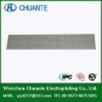
blue led pcb
原价: 180,00 USD
温州市, 中国

juanyang ye
联系人姓名
基本信息
| 出生地 | Zhejiang China (Mainland) |
|---|---|
| 牌子的名字 | ctpcb |
| 模式的数量 | ctpcb-13 |
related parater:Lead free HASL Surface finish required to meet ROHScompliant FR4 material with 0.4mm-3.0mm boards thickness Copper weight:0.5OZ,1OZ,2OZ 4-4mils track width spacing 0.2mm min finished hole size Technique Parameter: Surface processing typeHASL/ plating gold /immersion gold/ Ni/Au plating gold finger/OSP processing/immersion Tin (Sn)Layerssingle-sided,double-sidedMin trace width6milMin space width6milMin trace to pad/pad to pad space6milMin drill diameter0.2mmMin via pad0.6mmMax board size560mmX720mmMolding board thickness0.6-3.00mmMin solder mask dam6milMin solder mask clearance1.5milMin solder mask thickness10umSolder mask typeGreen/yellow/black/red/white/blue or transparent photosensitive solder mask and peel off blue glue.Min silk legend width6milMin silk legend height25milSilk legend colorWhite/ yellow /blackData file formatGERBER file and corresponding drilling file,PROTEL series,PADS2000,POWERPCB series,ODB++ Gerber file and Corresponding Broach file, PROTEL series,PADS2000,POWERPCB series, ODB++Electricity performance testing Electricity performance testing100% electrical performance testing,high pressure testing 100%electricity performance testing, high-pressure testingVarious types base material to PCB processingHigh TG board, high frequency board(ROGERS,TEFLON) halogen-free board (FR-4,CEM-1,CEM-3)Other testing requestImpendence testing, Hole resistance testing, gold slice up, Solder ability.
交货条款及包装
Packaging Detail: vacuum plastic and carton Delivery Detail: 3-10 working days
端口: Ningbo/Shanghai
付款条款
Letter of credit
Telegraphic transfer
Western Union
-
支付方式
我们接受:


