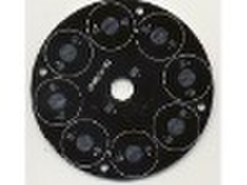
Aluminum PCB For LED
原价: 0,10 USD
深圳宝安国际机场, 中国

sunny ma
联系人姓名
基本信息
| 出生地 | Guangdong China (Mainland) |
|---|---|
| 牌子的名字 | HMY |
| 模式的数量 | JL-009 |
1,Our Product range We offer a wide range of PCBs such as single-sided, double-sided, multi-layer, high frequency, MCPCB, metal-backed PCB and so on. 2,Product quality Our factories got ISO9001, UL certificates and our products meet RoHS standards. 3,How can we help you? What we offer is better solutions,to help you inprove your quality while maintaining low production cost, but not just product. 4,Can I ask you three questions? (1),Do you have plans to import printed circuit board this year? (2),If so, do you have plan to find an supplier in China? (3),How can I Be a qualified supplier for you? And you could addme to your list if you need to find a new supplier, which is much appreciated that benefit to both of us. Please send me you Gerber files if our PCBs can meet your requirements, I will quote you the best price for your reference as soon as we receive your specific inquiry. Manufacture Capablity 1,Numbr of Layer 1-12Layers 2,Material FR-4,Taconic,Rogers, Teflon,High Tg CCL,Aluminium Base Board,Copper Base Board,Iron Base board,Metal-backed Laminate 3,Finish Board Thickness 0.2mm-4.5mm 4,Minimun Core Thickness 0.075mm(3mil) 5,Copper Thickness 1/2 oz min;5 oz max 6, Min.Trace Widty & Line Spacing 0.075mm/0.1mm(3mil/4mil) 7, Min.Hole Diameter for CNC Driling 0.25mm(12mil) 8,Min.Hole Diameter for punching 0.9mm(35mil) 9,Biggest panel size 610mm×508mm 10,Hole Positon +/-0.075mm(3mil) CNC Driling 11,Conductor Width(W) +/-0.05mm(2mil)or +/-20% of original artwork 12,Hole Diameter(H) PTH L:+/-0.075mm(3mil) Non-PTH L:+/-0.05mm(2mil) 13,Outline Tolerance +/-0.125mm(5mil) CNC Routing +/-0.15mm(6mil) by Punching 14,Warp & Twist 0.70% 15,Insulation Resistance 10Kohm-20Mohm 16,Conductivity <50ohm 17,Test Voltage 10-300V 18,Panel Size 110×100mm(min) 660×600mm(max) 19,Layer-layer misregistration 4 layers:0.15mm(6mil)max 6 layers:0.25mm(10mil)max 20,Min.spacing between hole edge to circuity pqttern of an inner layer 0.25mm(10mil) 21,Min.spacing between board oulineto circuitry pattern of an inner layer 0.25mm(10mil) 22,Board thickness tolerance 4 layers:+/-0.13mm(5mil) 6 layers:+/-0.15mm(6mil) 23,Impedance Control +/-10% 24,Different Impendance +-/10%
交货条款及包装
Packaging Detail: Inner: vacuumOuter:standard carton box Delivery Detail: 5-8 days
端口: Shenzhen,Hongkong
付款条款
Documents Against Acceptance
Documents Against Payment
Letter of credit
Telegraphic transfer
Western Union
-
支付方式
我们接受:


