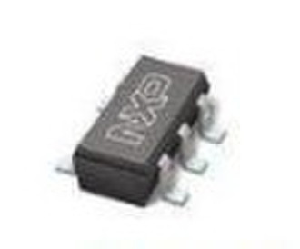
74LVC1G125GW - Bus buffer/line driver; 3-state - N
原价: 0,01 USD
深圳宝安国际机场, 中国
生产能力:
1000000 片 / 月

keiven wu
联系人姓名
基本信息
| 出生地 | Guangdong China (Mainland) |
|---|---|
| 牌子的名字 | NXP |
| 模式的数量 | 74LVC1G125GW |
NXP Semiconductors Product specification Bus buffer/line driver; 3-state 74LVC1G125 FEATURES · Wide supply voltage range from 1.65 V to 5.5 V · High noise immunity · Complies with JEDEC standard: – JESD8-7 (1.65 V to 1.95 V) – JESD8-5 (2.3 V to 2.7 V) – JESD8B/JESD36 (2.7 V to 3.6 V). · ±24 mA output drive (VCC = 3.0 V) · CMOS low power consumption · Latch-up performance exceeds 250 mA · Direct interface with TTL levels · Inputs accept voltages up to 5 V · Multiple package options · ESD protection: – HBM EIA/JESD22-A114-B exceeds 2000 V – MM EIA/JESD22-A115-A exceeds 200 V. · Specified from -40 °C to +85 °C and -40 °C to +125 °C. DESCRIPTION The 74LVC1G125 is a high-performance, low-power, low-voltage, Si-gate CMOS device, superior to most advanced CMOS compatible TTL families. The input can be driven from either 3.3 V or 5 V devices. This feature allows the use of this device in a mixed 3.3 V and 5 V environment. This device is fully specified for partial power-down applications using Ioff. The Ioff circuitry disables the output, preventing the damaging backflow current through the device when it is powered down. The 74LVC1G125 provides one non-inverting buffer/line driver with 3-state output. The 3-state output is controlled by the output enable input (OE). A HIGH level at pin OE causes the output to assume a high-impedance OFF-state. QUICK REFERENCE DATA GND = 0 V; Tamb = 25 °C; tr = tf £ 2.5 ns. Notes 1. CPD is used to determine the dynamic power dissipation (PD in mW). PD = CPD ´ VCC 2 ´ fi ´ N + S(CL ´ VCC 2 ´ fo) where: fi = input frequency in MHz; fo = output frequency in MHz; CL = output load capacitance in pF; VCC = supply voltage in Volts; N = total switching outputs; S(CL ´ VCC 2 ´ fo) = sum of the outputs. 2. The condition is VI = GND to VCC. SYMBOL PARAMETER CONDITIONS TYPICAL UNIT tPHL/tPLH propagation delay input A to output Y V
交货条款及包装
Packaging Detail: paper package Delivery Detail: 3days
端口: SHENZHEN
付款条款
Telegraphic transfer
MoneyGram
Western Union
-
支付方式
我们接受:


