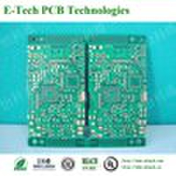
22 layers PCB board
原价: 0,20 USD
深圳宝安国际机场, 中国

Saya Liu
联系人姓名
基本信息
| 出生地 | Guangdong China (Mainland) |
|---|---|
| 牌子的名字 | EKT |
| 模式的数量 | PCB-P004 |
Our PCB got UL,SGS,ISO9002,RoHS,QS9000 and TS16949 certificates,and are used to a wide range of fields such as computers, digital products,medical equipment, automobiles, communication devices, military, industrial control and aviation. PCBprocess capability 1.layer: 2-22 layer 2.product type: Rigid PCB,High Density Inverter PCB,thick copper PCB 3.Materials: FR-4, CEM-3, Teflon, Aluminum Substrate, Rogers, Halogen Free, High Tg 4.Copper Thickness: 140micron(4oz) 5.Min Board Thickness: 0.4mm 6.Max Board Thickness: 5.0mm 7.Min finished Hole Diameter: 0.1mm 8.Outer layer line width / spacing: 0.1mm/0.1mm 9.Inner layer line width / spacing: 0.1mm/0.1mm 10.Min aperture: 0.2mm 11.Min Laser drilling: 0.1mm 12.Min Ring Width: 0.11mm 13.Min BGA-bit hole spacing: 0.4mm 14.Resistance Tolerance: ±10% 15.Minimum Insulation Thickness: 3mil 16.Maximum laser blind hole thickness to diameter ratio: 0.8:1 17.Maximum working board size: 520*622mm 18.Drilling Tolerance (PTH): ±0.075mm 19.Drilling tolerance (NPTH): ±0.05mm 20.Outline Tolerance (CNC): ±0.13mm 21.Surface coating: Lead Free HASL,Immersion Gold, Immersion Tin, Immersion Silver, OSP, Gold Finger Plating, Carbon Ink Printing, Peelable Blue Mask PCB production capacity Double sided PCB :200000 ft2 /Month Multilayer PCB :320000 ft2/Month HDI PCB : 80000 ft2/Month
交货条款及包装
Packaging Detail: pcb Vacuum package,Seal package Delivery Detail: 3-10 days
端口: Shenzhen\HK
付款条款
Letter of credit
Telegraphic transfer
Western Union
-
支付方式
我们接受:


